Tag Archive: pdf


Image

  The following CD4017 circuits have not been tested and is presented here as a possibility only. If you experiment with this circuit, please send me any problems found so that the circuit can be updated.

  The following circuits are designed to change the duration of each positive output pulse from the astable timer. The circuits use a CD4017 Decade Counter / Decoder to provide nine or ten steps in the cycle.

  The first circuit operates with a repeating ten step cycle. Each output pulse is longer than the previous until a count of ten is reached at which time the cycle will repeat.

  The second circuit has a nine step cycle that stops at the end of the cycle. The cycle is restarted or reset when the RESET input is briefly made high.

  The CD4017 can be configured to give count lengths between 1 and 10. Refer to the timing diagram in the CD4017 data sheet for a better understanding of the IC’s operation.

The MAX705CSA is a microprocessor (μP) supervisory circuit which reduces the complexity and number of components required to monitor power-supply and battery functions in μP systems. The device significantly improves system reliability and accuracy compared to separate ICs or discrete components. The applications of the MAX705CSA include Computers, Controllers, Intelligent Instruments, Automotive Systems, Critical μP Power Monitoring.
 Image
MAX705CSA absolute maximum ratings: (1)VCC: -0.3V to 6.0V; (2)All Other Inputs: -0.3V to (VCC + 0.3V); (3)Input Current, VCC: 20mA; GND: 20mA; (4)Output Current (all outputs): 20mA; (5)Continuous Power Dissipation, Plastic DIP (derate 9.09mW/℃ above +70℃): 727mW.
 
MAX705CSA features: (1)μMAX Package: Smallest 8-Pin SO; (2)Guaranteed RESET Valid at VCC = 1V; (3)Precision Supply-Voltage Monitor, 4.65V in MAX705/MAX707/MAX813L; 4.40V in MAX706/MAX708; (4)200ms Reset Pulse Width; (5)Debounced TTL/CMOS-Compatible Manual-Reset Input; (6)Independent Watchdog Timer—1.6sec Timeout (MAX705/MAX706); (7)Active-High Reset Output (MAX707/MAX708/MAX813L); (8)Voltage Monitor for Power-Fail or Low-Battery Warning.

I know how to build a big digit but how the heck did you control that much current with such few ICs and such few control lines? Ahh, I’m glad you asked. Here are some fun pointers about how to control large numbers of seven segments LEDs.

Now if you’re not a hardware person, get ready for some technical jargon.

A PIC 16F877A has quite a few I/O pins (around 32). But if you start doing the math, you see just how limited we are.

6 digits * 7 segments = 42 channels

Sure, we could find a microcontroller that has 42 available I/O pins, but there’s got to be a better way! This is actually an age-old problem. Turns out there are chips out there! The 74HC4511 is the magical chip that takes a Binary-Coded-Decimal (BCD) input and outputs the correct pins to create that binary number on a seven-segment display.

Okay, so we go from seven lines down to four, big deal? There is a latch on the 74HC4511. This latch allows us to share the 4-bit bus with all the channels, and then just toggle the latch pin on the digit we need to talk to. Maybe a schematic will help:

Image

You can see four Control lines. This is the BCD bus. There is also six Driver lines. These Driver lines activate the latch on each ‘channel’.
Image

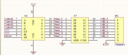
U6 is the 74HC4511. U7 is a ULN2003A. JP1 is the RJ45 jack. Just stick with me a bit longer!

The ULN2003A is a high-current Darlington array. Darling what? This IC has seven channels. Each channel can control up to 500mA. When 1B goes high, current is allowed from the ‘1C’ input to ground.

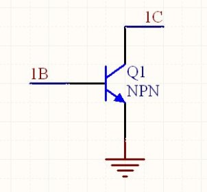
So when the Num1_f pin goes high, current flows from RAW, through the LED Light Bars in the big digit, into 1C, and then out through GND. This may seem a little bit odd at first. Maybe this will help:
Image

Okay so now for the chain of events.

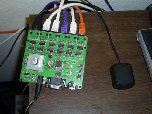
The PIC parses out the GPS time from NMEA sentences coming out of the Lassen iQ receiver at 4800bps.
The PIC decides that the time is 6:45:33, so a ‘3’ needs to be displayed on channel 1.
A binary three (0b.0011) is put onto the bus.
Driver1 is pulled low, then driven high. Because all other driver lines are kept high, the other drivers ignore this bus data.
The 74HC4511 for channel 1 sees this binary number, notices that it’s been latched, and then outputs the correct segments to light up a three. Segments A, B, C, D, and G go high.
The ULN2003A detects these lines (Num1_a, b, c, d and g), goes high and allows current to sink through 3C, 4C, 5C, 6C, and 2C.
The LED Light Bars inside the digit (located farthest to the right) light up the correct bars to display a three.

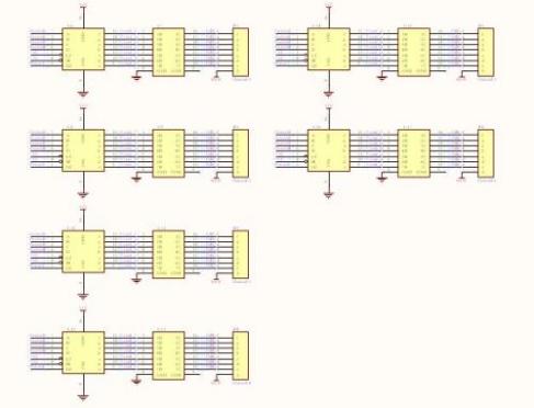
It’s really pretty slick. The system is completely scalable. To add another seven-segment display requires only one additional I/O pin for another DriverX line. The PIC 16F877A could control as many as 28 digits. Have you ever seen 28 digits next to each other? How about 18″ wide and on a wall? That’s really huge.
Image24

That’s it! Sorry the tutorial ended up being so long. This project took about two weeks of cutting and figuring out how to best create the digits. The firmware took about an hour and hardware layout took about three (we’ve used most of the basic components before). Let us know what you think.

HI, I’m working on a circuit that uses two 555 timers. At the electronics store, they gave me a handful of 555 chips, I only noticed the difference when I finished my circuit: the R1 value is shorted out, my R2 value is 150 Ohms, and the electrolytic cap is 10 uF. (see the schematic with R3, D1 and D2 replaced with a single piezo speaker).

ImageThe thing is, if I put in the 555 chip marked LM555CN, it appears to be ‘always on’. But, if I use the Texas Instruments chip marked NE555P, the circuit works as expected, that is, it generates an annoying screech on a piezo speaker. What is the difference between these two seemingly identical chips? Is it a quirk in the TI chip that it works when R1 is just shorted out? And lastly, is there a way around this problem other than me sitting at the electronics store picking out the TI chips?

Also note – the piezo speaker doesn’t have any oscillator in it, that is, when you apply raw power to it, it just clicks once and sits there, that’s why I have the second 555 timer, and it’s not an option to change out the speakers at this point.

MAX232CSE line driver/receiver

Image
The MAX232CSE line driver/receiver is intended for all EIA/TIA-232E and V28/V24 communications interfaces, particularly applications where ±12V is not available. These parts are especially useful in battery-powered systems, since their low-power shutdown mode reduces power dissipation to less than 5μW. The MAX232CSE uses no external components and are recommended for applications where printed circuit board space is critical.
 
MAX232CSE absolute maximum ratings: (1)Supply Voltage (VCC): -0.3V to +6V; (2)V+: (VCC – 0.3V) to +14V; (3)V: +0.3V to +14V; (4)Input Voltages; (5)TIN: -0.3V to (VCC – 0.3V); (6)RIN (Except MAX220): ±30V; (7)RIN (MAX220): ±25V; (8)TOUT (Except MAX220): ±15V; (9)TOUT (MAX220): ±13.2V; (10)Output Voltages; (11)TOUT: ±15V; (12)ROUT: -0.3V to (VCC + 0.3V); (13)Driver/Receiver Output Short Circuited to GND: Continuous; (14)Storage Temperature Range: -65℃ to +160℃; (15)Lead Temperature (soldering, 10s): +300℃.
 
MAX232CSE features: (1)For Low-Voltage, Integrated ESD Applications MAX3222E/MAX3232E/MAX3237E/MAX3241E/MAX3246E: +3.0V to +5.5V, Low-Power, Up to 1Mbps, True RS-232 Transceivers Using Four 0.1μF External Capacitors; (2)For Low-Cost Applications MAX221E: ±15kV ESD-Protected, +5V, 1μA, Single RS-232 Transceiver with AutoShutdown.

ICL7107CPL Pinout

This is one package pinout of ICL7107CPL,If you need more pinouts please download ICL7107CPL’s pdf datasheet.
Image